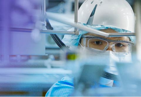
We have been an innovation leader for 50 years. We not only contribute to the remarkable advance of the semiconductor industry, we help shape the industry itself through our collaborative research and development (R&D) models. This success, and our future success, is largely dependent on our ability to develop new products and new materials, and to improve existing products and materials. Achieving this requires a large commitment to R&D. In 2017 and 2016, our R&D investments were €114 million and €102 million respectively. As of year-end 2017, 497 employees were employed in R&D, representing 26% of our total staff.
.png)
As a global company, we carry out R&D on different continents, giving us access to the smartest professionals working in the semiconductor sector today, and bringing our R&D closer to our customers. In our research centers in Belgium, Finland, Japan, the Netherlands, South Korea, and the United States we are active at all stages of our innovations’ life cycle, from developing the basic chemistry and materials to implementing improvements on our equipment at our customers’ production sites. We also work with specialists across a wide array of disciplines to develop our research goals, including scientists from research institutes, universities, and suppliers.
With our R&D activities chiefly conducted in the principal semiconductor markets of the world, we are able to draw on innovative and technical capabilities internationally. Each geographical center provides expertise for specific products or technologies, and interacts with customers on a global scale. This approach, combined with structured and managed interactions between the individual centers, enables the efficient allocation of resources during development and knowledge sharing.
Under the umbrella of our global product development policies, our local activities are directed both towards expanding and improving existing product lines to incorporate technology improvements and reduce product cost and total cost of ownership, as well as developing new products for existing and new markets. These activities require the application of physics, chemistry, materials science, electrical engineering, precision mechanical engineering, software engineering, and systems engineering.
The most important collaborations we have are those with our customers, with whom we co-create and jointly develop technology roadmaps, and new processes and materials when our customers need them for their next products. The diversity in collaborations ranging from early research to pilot production helps us reduce risk as early as possible in the innovation life cycle.
A global platform engineering group addresses the needs for common platforms for the various products in our product portfolio. This helps us in driving standardization of hardware and software through the organization. A corporate R&D group consisting mainly of resources in Leuven, Belgium and Helsinki, Finland addresses common needs for advanced process and materials development, and process integration work for the 5nm, 3nm and 2nm nodes, and even beyond.
| Location | Number of R&D employees as of December 31, 2017, exclusive of temporary workers | |
| Almere, the Netherlands | 35 | |
| Leuven, Belgium | 28 | |
| Helsinki, Finland | 27 | |
| Phoenix, Arizona, United States | 194 | |
| Cheonan, South Korea | 92 | |
| Singapore | 4 | |
| Tokyo, Japan | 117 | |
| Total | 497 |
As part of our research and development activities, we are engaged in various formal and informal arrangements with customers, suppliers, research institutes and universities.
Next to large scale R&D engagements, we have specific bilateral research activities with several key academic groups at universities in Asia and Europe, typically centric to our core R&D focus on new equipment, material and process developments.
We contribute to several process and equipment development projects at the major Dutch technical universities through the Dutch FOM and STW funding organizations for fundamental and applied research.
We participate in select publicly-funded programs to research and develop technology for semiconductor devices with line widths of 5nm and below, and in ‘More than Moore’ technologies. We are also involved in several cluster development programs in the Eureka initiative, as a member of the AENEAS association as mentor or reviewer, and in road-mapping activities.
And finally, we occasionally cooperate with other semiconductor capital equipment suppliers in complementary fields, in order to gain knowledge on the performance of our own deposition processes, in cooperation with other processes, either in bilateral or consortia projects.
We expect new deposition technologies and chemistries to be a major driver for new intellectual property (IP) in the future. Patents protect our discoveries and enable us to speak more openly about our inventions and share ideas in the marketplace that benefit our customers. Our patents are usually registered in the principal countries where semiconductor devices or equipment are manufactured and/or sold. Our vision is to increase our value to our customers and shareholders by using our IP in a way that differentiates our products, influences the market, and provides additional monetization opportunities.
We have been an innovation leader within the semiconductor industry for 50 years. During that time, we have helped shape the industry through a series of breakthrough innovations in technologies such as ALD, plasma deposition, and epitaxy.
We strive to maintain a culture of innovation at every level of the organization. We attract and retain creative people from around the world, who help us create a steady stream of innovations that we bring to volume manufacturing through close cooperation with our customers.
Our vision is to increase value to the company and our customers through innovations and the use of our IP to differentiate our products. We understand that a failure to adequately protect our IP and/or leakage of our IP could result in the loss of our competitive advantage and adversely impact demand, as well as our financial performance.
We have implemented a robust IP protection program that protects IP for us, our customers, our suppliers and our partners. We train all employees not only on the importance of IP protection, but also on how to recognize and report possible IP infractions. This training is provided to all new hires, and employees are given regular refresher training.
We continue to implement new software, training, and agreements which will allow us to better protect our IP and safeguard our technology developments.
Our technologies, innovations, IP, products and process data, as well as the sensitive information about our customers, suppliers, and employees, are valuable assets. Any breach of our information systems could adversely affect our finances and operating results, as well as our reputation. Information security is a material aspect to us and our stakeholders, and requires the proper controls to protect it.
Our approach to information security management includes developing and sustaining a proper global IT security management framework with a policy, processes, and controls to protect against unauthorized system access and loss of valuable information, regardless of location.
In 2017, we continued to assess our position on network security and took steps to enhance the security posture of our global network, improved employee education, and awareness on cyber security/safety, and made infrastructure modernization enhancements.
Our goal is to protect our intellectual property and privacy, while mitigating risks and achieving data security for our customers, employees, and other stakeholders.
We keep shrinking
dimensions by developing
new solutions to advance
Moore’s law.


